Sahasra Semiconductors Inaugurates Rajasthan’s First Semiconductor Plant

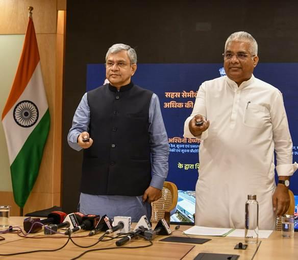 The Electronics Manufacturing Cluster (EMC) developed by ELCINA at Salarpur, Khushkhera, Bhiwadi, Rajasthan, along with the Semiconductor ATMP/OSAT facility of Sahasra Semiconductors Pvt Ltd, was virtually inaugurated by Union Minister for Electronics & Information Technology Shri Ashwini Vaishnaw. The inauguration took place in the presence of Bhajan Lal Sharma, Chief Minister of Rajasthan and Bhupender Yadav, Union Minister for Environment, Forest and Climate Change.
The event marks a significant milestone in India’s journey towards becoming a global hub for electronics manufacturing and semiconductors. This progress is being driven by the visionary initiatives of ‘Make in India’, ‘Digital India’ and ‘Atmanirbhar Bharat’, launched under the leadership of Prime Minister Narendra Modi.
Addressing the gathering, Vaishnaw called this a historic day for the state of Rajasthan as it enters the semiconductor industry—a strategically critical industry globally from a geopolitical perspective.
He highlighted India’s rapid progress in electronics manufacturing over the last 12 years, with production growing 6 times to nearly INR 13 lakh crore and exports rising to around INR 4.24 lakh crore. He underscored that mobile phones have now become India’s top export commodity.
The Union Minister credited this to Prime Minister Narendra Modi’s treatment of electronics and semiconductors as focus sectors. He added that schemes like Electronics Component Manufacturing Scheme (ECMS), Electronics Manufacturing Clusters (EMC), India Semiconductor Mission (ISM), and Production Linked Incentives (PLI) are implemented methodically by working together with the state Governments and industries.
Rajasthan Chief Minister underlined that the State Government has in March 2026 come out with a Rajasthan Semiconductor Policy and outlined his priority to develop the region close to Delhi NCR into a manufacturing hub. Union Minister Yadav also noted that earlier, Bhiwadi region was known mainly for the automobile sector, but now semiconductor and electronics industries are also being promoted.
ELCINA Electronics Manufacturing Cluster (EMC)
This cluster at Bhiwadi has been developed over 50.3 acres with a project cost of INR 46.09 crore. Government of India has provided a direct support of INR 20.24 crore under the EMC scheme. The cluster has been established by M/s ELCINA Electronics Manufacturing Cluster Pvt Ltd (SPV), a joint collaborative initiative of MSME industry players under the banner of ELCINA.
It is equipped with world-class infrastructure including uninterrupted power and water supply, internal roads, centralized administrative facilities, testing and training centres, and a dedicated Skill Development Centre with smart classrooms and laboratories.
The cluster is strategically located near the National Capital Region with strong road, rail, and air connectivity. With this the cluster is expected to emerge as a major destination for electronics component manufacturing.
The EMC has already attracted planned investments of over INR 1,200 crore by 20 companies. These companies are engaged in sectors ranging from semiconductor packaging and electronic components to air conditioners, RFID technologies, EV parts, and industrial electronics. Eleven companies are currently operational with cumulative investments of over INR 900 crore, generating employment for over 2,700 persons.
Among the major companies operational in the cluster are Aisan Fiem Industries, E-Pack Durable, Sahasra Semiconductor, Sahasra Electronics, Varada Green Energy, Duggar Power Products and the Electronics Sector Skill Council of India, etc.
Semiconductor ATMP/OSAT Facility
This facility of M/s Sahasra Semiconductors Pvt Ltd is India’s 1st Small and Medium Enterprise (SME) to start commercial production of semiconductor chips. Developed under MeitY’s Scheme for Promotion of Manufacturing of Electronic Components and Semiconductors (SPECS), the facility has been set up with an investment of over INR 150 crore. It is spread over 57,000 sq ft and equipped with Class 10K and 100K cleanrooms. The facility will package memory chips for products such as Micro SD and flash storage, along with LED driver ICs, eSIMs, and RFID products.
The unit currently has an annual packaging capacity of 60 million semiconductor units with SPECS-supported projected capacity of about 43 million units. It has plans to scale up to nearly 400-600 million units annually over the next 2–3 years.
The facility is already exporting more than 60 percent of its production to global markets, including the United States, Germany, France, Eastern Europe, China, and Nepal. The facility is now moving towards its own product R&D, including LED driver chips and other semiconductor products. It will also support training of youth in semiconductor packaging and high-tech manufacturing in collaboration with ESSCI and technical institutes.
For more information: www.pib.gov.in